
How Are Magnetic Lenses in SEMs Redefining Precision in Semiconductor Metrology?
Semiconductor Metrology Series – 1

Advanced Magnetic Technology in SEMs: Enhancing Semiconductor Metrology
As semiconductor devices continue to shrink and grow more complex, the demand for cutting-edge metrology tools has never been greater. Scanning Electron Microscopes (SEMs), which play a vital role in modern semiconductor processes, rely on magnetic technology to deliver high-resolution imaging and detailed analysis.
The Role of Magnetic Lenses in SEMs
Magnetic lenses are essential components within SEMs, focusing and controlling the electron beam with unparalleled precision. Beyond enhancing image clarity, they ensure that every critical dimension, surface defect, and microscopic feature is measured with exceptional accuracy.
Primary Applications of Scanning Electron Microscopes (SEMs)
SEMs are widely used for high-resolution imaging and analysis of surface topography, composition, and material microstructure at the nanoscale. In semiconductor metrology, SEMs are critical for:
- Critical Dimension (CD) Measurement: Measuring line widths, spaces, and other features on wafers to meet design specifications.
- Defect Inspection: Detecting and classifying surface and sub-surface defects like particles, voids, and cracks that can impact device performance.
- Surface Analysis: Evaluating surface roughness, texture, and morphology, which are essential for device reliability.
- Failure Analysis: Providing detailed images of failed regions to diagnose issues in semiconductor devices
How SEMs Work in Semiconductor Metrology
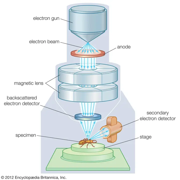
SEMs function by directing a focused beam of high-energy electrons onto a sample surface. The interaction generates signals that form an image or reveal composition details. Key SEM components include:
- Electron Gun: Produces a high-energy electron beam (0.1 to 30 keV).
- Electromagnetic Lenses: Focus and control the beam for high precision.
- Scan Coils: Move the beam across the sample in a raster pattern.
- Detectors: Capture signals (secondary electrons, backscattered electrons, X-rays) for imaging and analysis.
- Vacuum Chamber: Maintains a high-vacuum environment to prevent electron scattering.
Magnetic Lenses: The Core of SEM Precision
Magnetic lenses play a crucial role in SEMs, using magnetic fields generated by electromagnets to focus and control the electron beam. Their design directly impacts the resolution and accuracy required for semiconductor metrology.
Key Considerations in Magnetic Lens Design
- Magnetic Field Uniformity: A uniform magnetic field is essential for precise focusing. Any distortions can reduce image quality and measurement accuracy.
- Aberration Control: Minimizing spherical and chromatic aberrations is critical for high-resolution imaging. Optimized lens geometry and materials help achieve this.
- Thermal Stability: Consistent magnetic field strength is maintained through proper cooling systems and material selection to prevent focus drift.
- Material Selection: Soft magnetic alloys with high permeability and low hysteresis loss are chosen for efficient magnetic field generation and minimal energy loss.
- Precision Assembly: Precise winding of coils and careful assembly of electromagnets are vital to achieving optimal magnetic field characteristics.
Conclusion: Pushing the Limits of SEM Technology with Dexter Magnetic Technologies
Magnetic technology is at the heart of SEM performance, and magnetic lenses play a critical role in achieving the high-resolution imaging and precise measurements essential for semiconductor metrology. At Dexter Magnetic Technologies, we’re leading the charge in developing advanced magnetic solutions that enhance semiconductor manufacturing processes.